Context
-
Union Minister of State for Electronics & Information Technology and Skill Development & Entrepreneurship, Rajeev Chandrasekhar visited the Gallium Nitride Ecosystem Enabling Centre and Incubator ( GEECI ) facility at the prestigious Indian Institute of Sciences (IISc), Bengaluru.
-
The facility has been jointly set up by Ministry of Electronics and Information Technology and IISc Bengaluru aimed at establishing GaN based Development Line Foundry facility, especially for RF and power applications, including strategic applications.
Key Details
- Gallium Nitride (GaN) to play a key role in enabling e-vehicles and wireless communication.
- Gallium Nitride Technology is of strategic importance with its application to 5G, space and defense application.
- There is tremendous opportunity in the electronics manufacturing & in the field of electronics and semiconductor design.
- Along with PLI and DLI schemes, GaN ecosystem will drive the innovation and encourage startups and entrepreneurs to look into business and technology seriously in next two years.

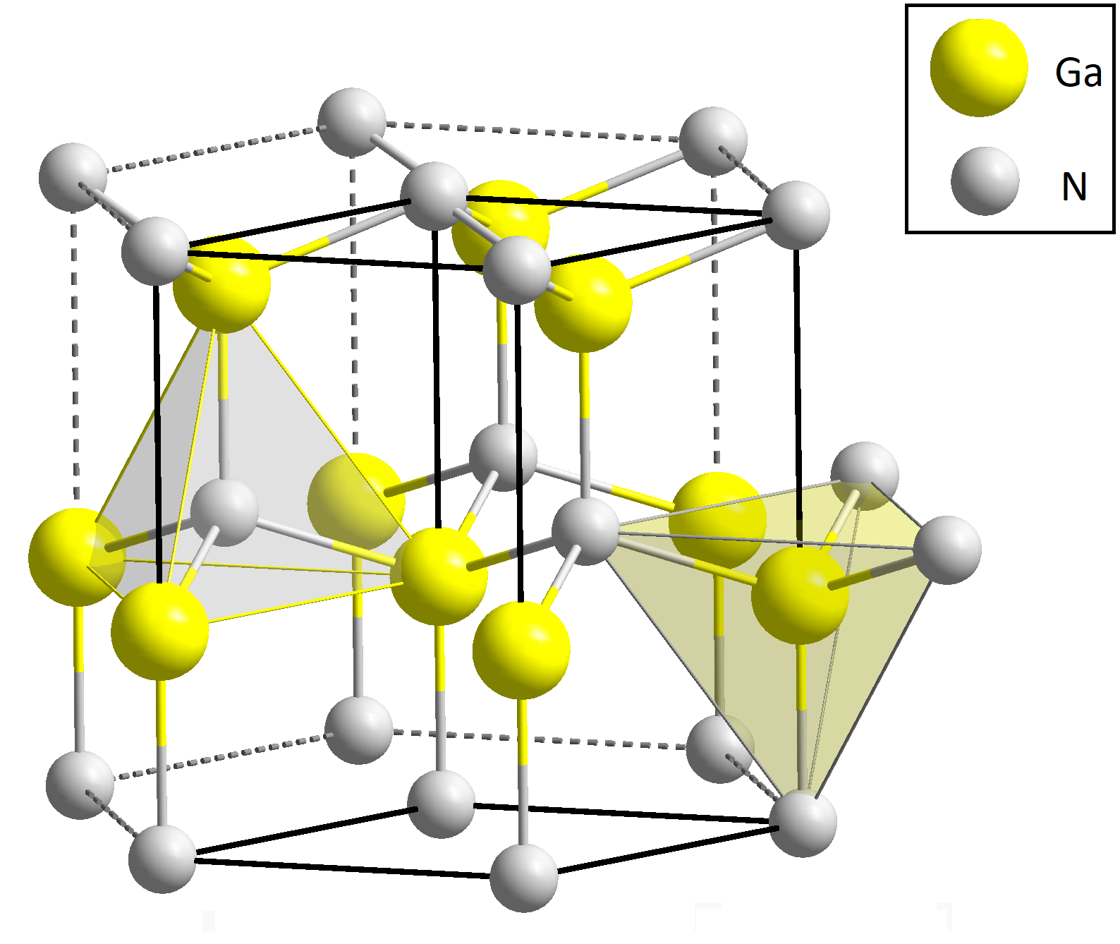
Credit: Wikipedia - AGNIT Semiconductors Pvt. Ltd. the first startup has already been incubated in TBI-InCeNSE an incubator of SID, IISc. It has raised its first round of angel funding. This will be the first startup to leverage the infrastructure created by GEECI.
Back to Basics
About Gallium Nitride (GaN)
- Gallium Nitride is a binary III/V direct bandgap semiconductor.
- It is very hard and mechanically stable.
- It is well-suited for high-power transistors capable of operating at high temperatures.
- Since the 1990s, it has been commonly used in Light Emitting Diodes (LED).
- Gallium nitride gives off a blue light used for disc-reading in Blu-ray.
- Additionally, gallium nitride is used in semiconductor power devices, RF components, lasers, and photonics.
- In the future, we will see GaN in sensor technology.
- Its sensitivity to ionizing radiation is low (like other group III nitrides), making it a suitable material for solar cell arrays for satellites. Military and space applications could also benefit as devices have shown stability in radiation environments.
- Because GaN transistors can operate at much higher temperatures and work at much higher voltages than gallium arsenide (GaAs) transistors, they make ideal power amplifiers at microwave frequencies.
- GaN is the substrate which makes violet (405 nm) laser diodes possible, without requiring nonlinear optical frequency-doubling.
- Advantages:
- Reduced energy costs
- Higher power density (smaller volume)
- Higher switching frequency
- Lower system cost
Reference:
https://www.pib.gov.in/PressReleasePage.aspx?PRID=1805535
Visit Abhiyan PEDIA (One of the Most Followed / Recommended) for UPSC Revisions: Click Here
IAS Abhiyan is now on Telegram: Click on the Below link to Join our Channels to stay Updated
IAS Abhiyan Official: Click Here to Join
For UPSC Mains Value Edition (Facts, Quotes, Best Practices, Case Studies): Click Here to Join
